This page describes the implementation of (Yet Another) avalanche noise hardware random number generator. This is a device which has been implemented many times [e.g. Rob Seward, Aaron Logue], including some commercial offerings [e.g. Entropy Key, TrueRNG]. This project does not do anything better than existing work, but I learned a lot.
Theory
This True Random Number Generator (TRNG) is based on avalanche breakdown noise in a PN junction. A PN junction is a semiconductor structure which forms a diode, allowing (ideally) electric current to flow in only one direction. Electric fields internal to the structure support a potential gradient allowing current to flow easily in one direction but creating a potential barrier for electrons driven in the reverse direction.
If strongly reverse-biased, however, electrons which overcome that potential barrier can have sufficient energy to cause impact ionization, leading to a multiplication effect1. An energetic electron impacting a silicon atom in the lattice can knock another electron out of the valence band (forming another electron-hole pair). In the presence of a strong reverse-biased electric field (needed to initiate this process in the first place), the liberated electron will accelerate and the process can continue, creating something like a sustained chain reaction.
Laying aside quantum effects and considering electrons in our PN junction to act as a Newtonian gas, avalanche breakdown is formally a chaotic process: It depends upon strongly nonlinear interactions between a large number of elements and exhibits topological mixing (the charge carriers mix throughout the structure and effects are not localized). Chaos means that this system, even if theoretically deterministic (I believe it is not), is highly sensitive to a tremendously large and unknowable set of initial conditions, rendering it unpredictable.
Prototype
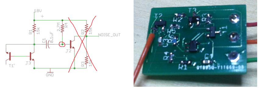
The prototype is based upon a design by Will Ware. The physical random source is a reverse-biased PN junction (actually two terminals of a bipolar junction transistor). Part of a transistor is used, rather than a diode, because diodes are typically designed with either very high breakdown voltage (as in the case of rectifying diodes) or low breakdown voltages but with minimal avalanche noise (e.g. zener diodes which are meant to be used in breakdown). A schematic is shown below.
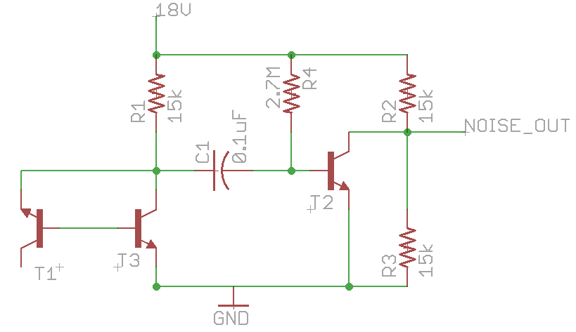
The PN junction formed by the base and emitter of T1 is reverse-biased by an 18V source (realized by two 9V batteries). The collector is left floating. The output is amplified by common-emitter amplifier T3 and coupled through C1 to another common-emitter stage (T2).
I constructed this prototype on perfboard and sampled the output using the ADC on-board an Arduino Uno. After correcting the output distribution using Von Neumann’s algorithm, the effective data rate was around 1000 random bits per second, and the device passed the diehard suite of statistical tests.
With a working prototype, I set out to create an integrated PCB, increase the data rate, and replace the Arduino with a USB interface.
Iteration 1: PCB 1, power supply
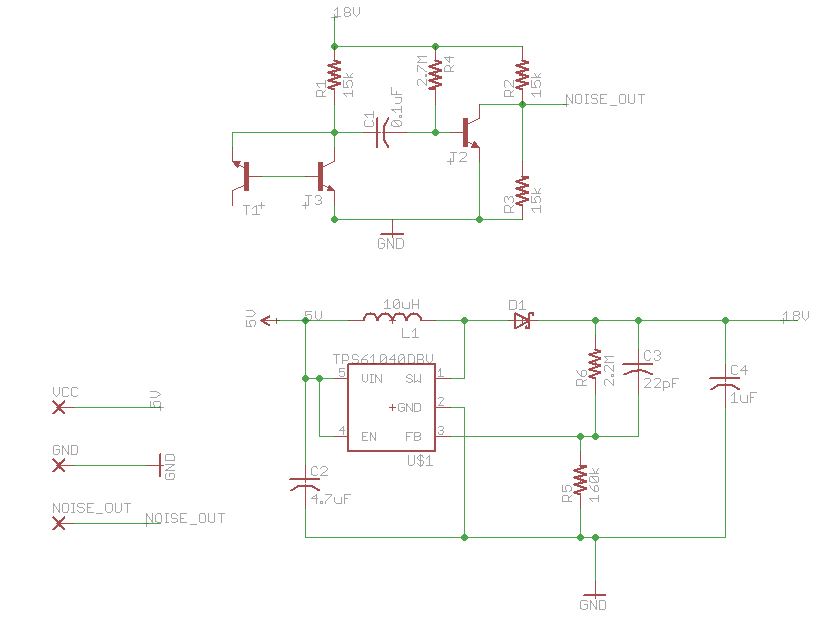
The first iteration adds an 18V supply based on the Texas Instruments TPS61040 DC/DC boost converter designed for LCD and LED display lighting applications. The datasheet contains a reference design (Figure 16, pg. 14) for an 18V output from a 5V supply. This eliminates the 9V batteries and allows the design to be powered from USB.
A PCB was created (using the free version of EAGLE) containing the power supply, physics package, and amplifiers. I used 0603 passives and replaced the through-hole 2N3904 transistor from the prototype with the MMBT3904, a surface-mounted equivalent.
The PCB was manufactured by Seeed Studio Fusion, a low-cost PCB service. It was assembled and tested with the Arduino.
Iteration 2: PCB 2, ADC and LPC1343
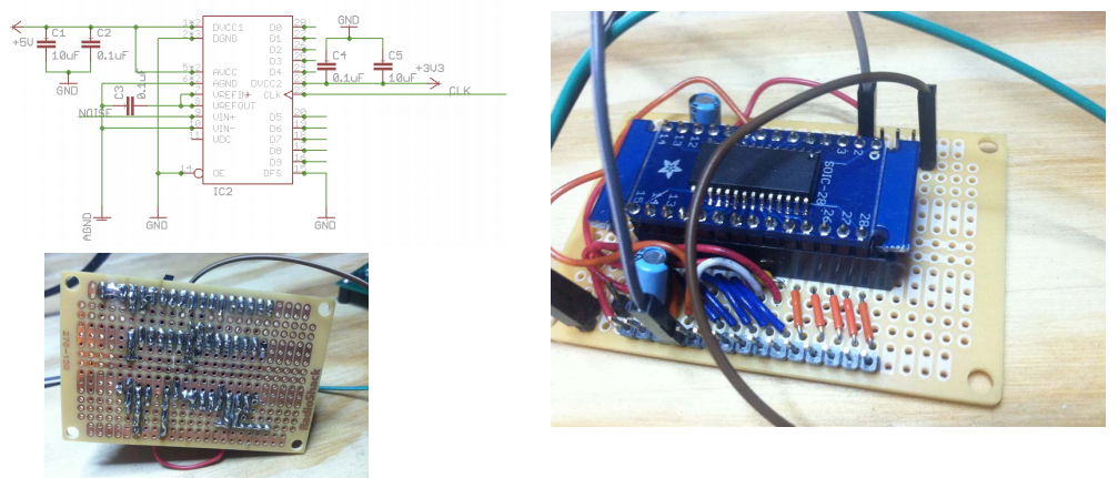
Next, I needed a faster interface. After some research I chose to use the LPC1343, a 32-bit ARM Cortex-M3 microprocessor which has a native USB interface and runs at up to 72 MHz. Olimex offers a LPC1343 dev board with published schematics. Using the LPC1343’s on-board ADC, I was able to get about a 40x speedup over the Arduino.
I adapted reference USB mass storage code for the LPC1343 and created a virtual mass storage interface for the device (this is not ideal). When inserted, the TRNG enumerates as a mass storage device (e.g. a USB thumbdrive) of arbitrary capacity. It would appear to, e.g. Linux, as a block device. Writes do nothing and return success. Reads return blocks of random data sampled from the noise circuit.
Next, I found the Intersil HI5767/2CBZ, a fast (up to 20 megasamples per second) dedicated 10-bit ADC in a SOIC-28 package. Driving the ADC at the LPC1343’s clock frequency (12 MHz) led to an overall speedup of 400x vs the prototype.
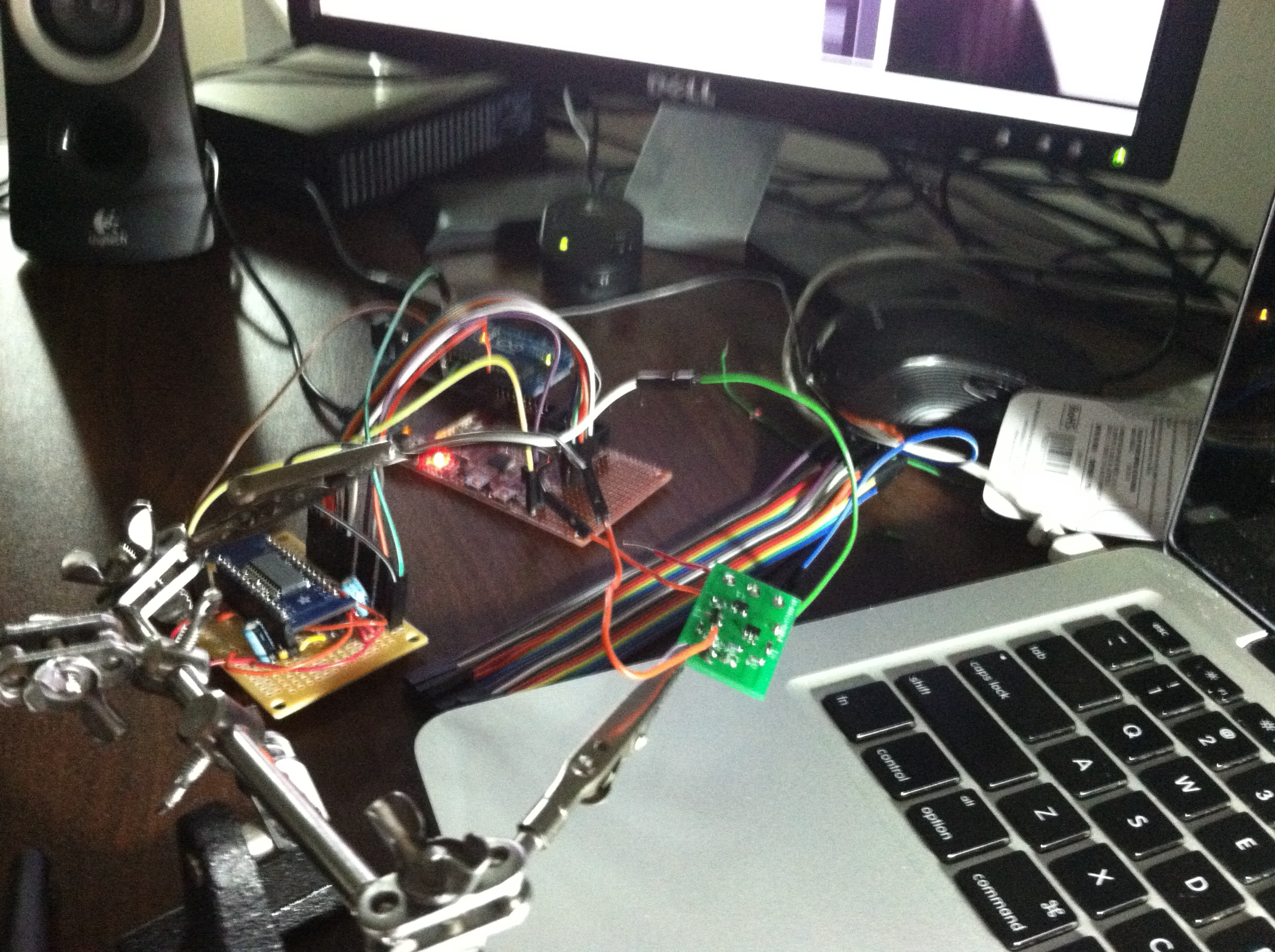
I created a SSOIC-28 breakout board using a PCB from Adafruit and built a test circuit for the ADC on perfboard (pictured below), following a reference schematic in the HI5767 datasheet (Figure 19, pg. 13).
The HI5767 has an input dynamic range of no more than 1Vp-p, and I found that removing the second amplifier from the amplifier chain in my physics package reduced the output to within this level. I was able to hack the PCB (pictured below) to achieve this, saving me considerable time.
The test setup, shown below, consists of the Arduino Uno (now providing only a 5V power supply!), the LPC1343 (providing a USB interface), The physics package PCB #1 from above (hacked for 1V output), and my ADC test circuit. It is a mess.
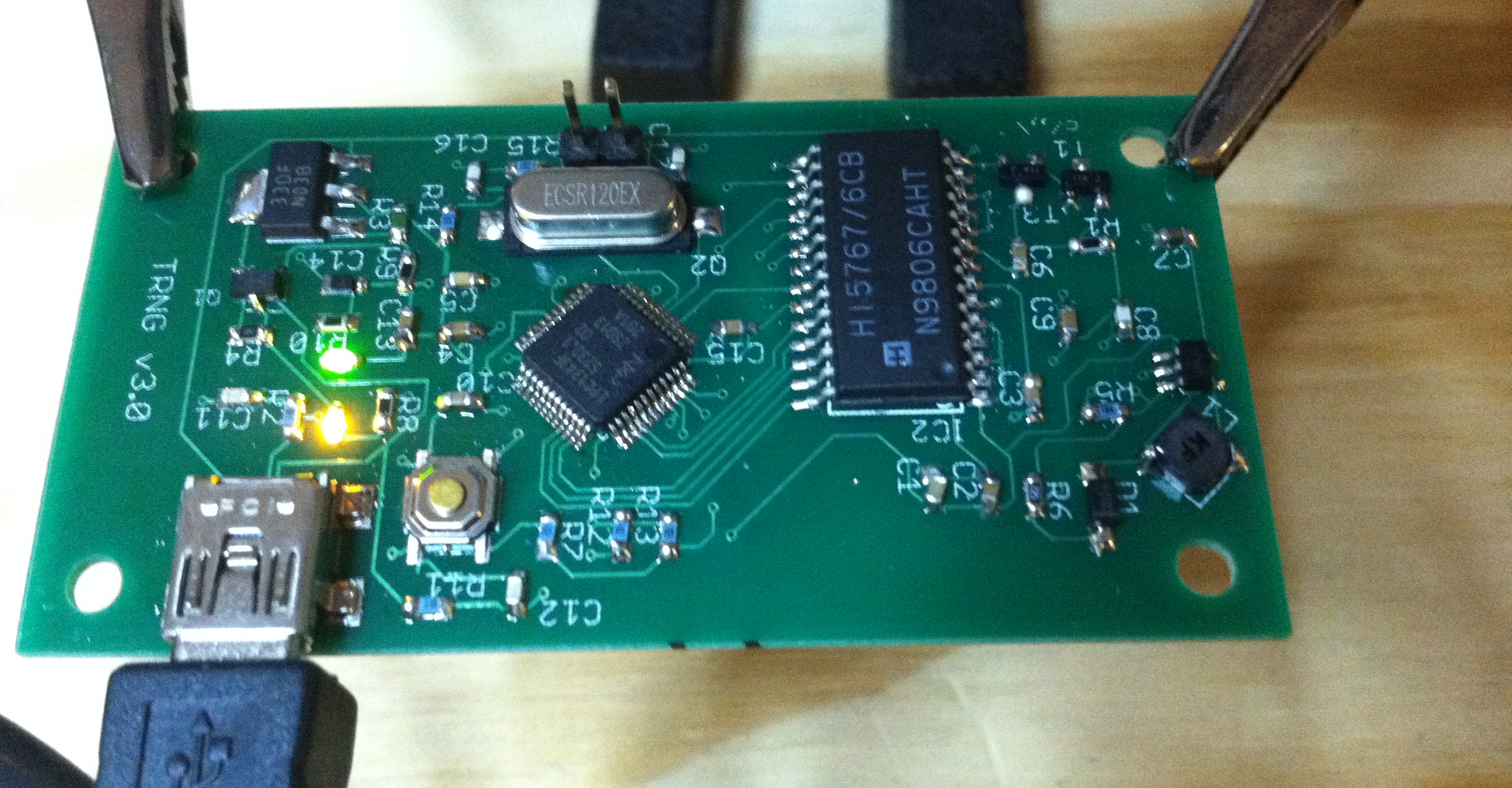
Iteration 3: Integration
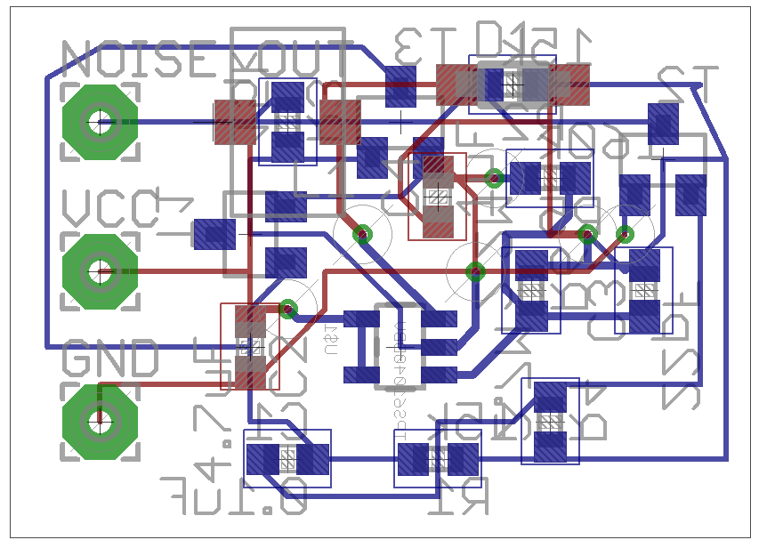
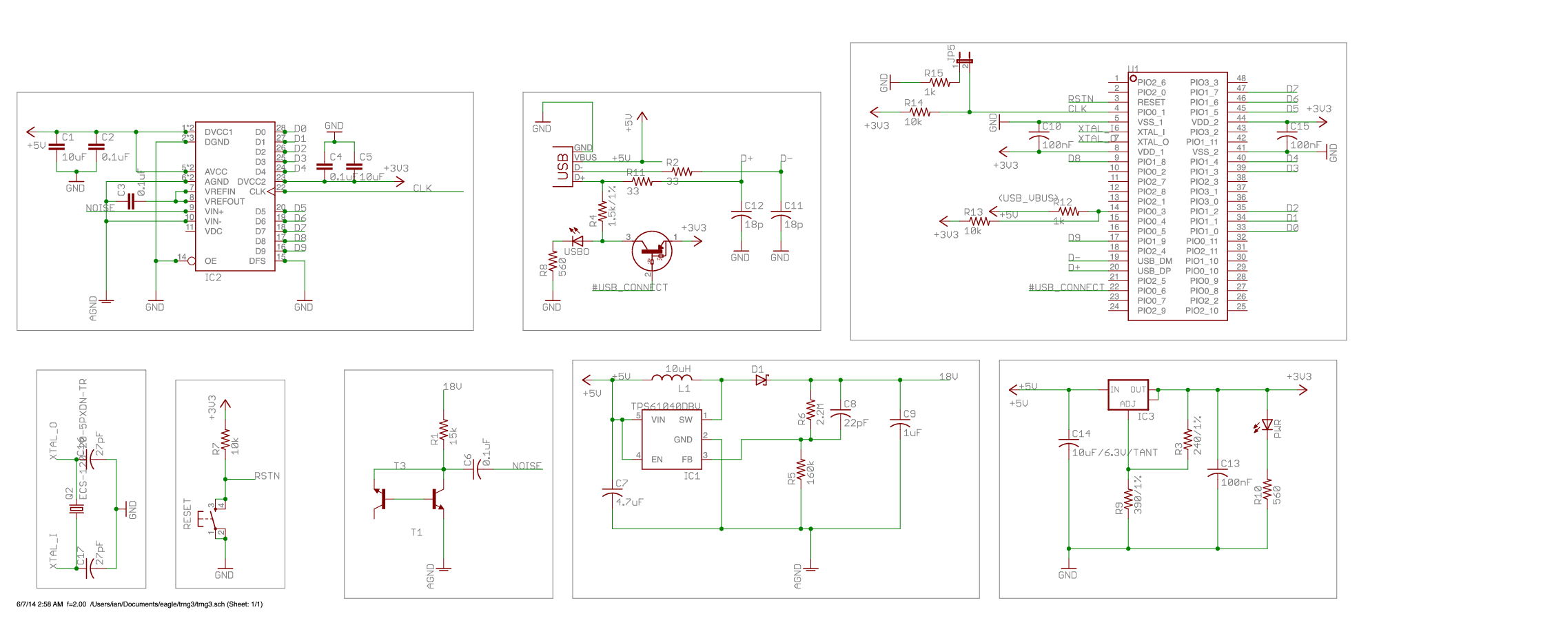
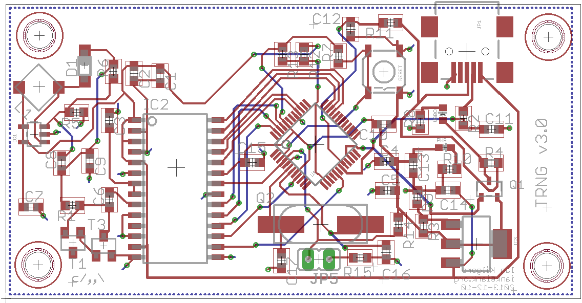
Finally, I created a single integrated PCB. I attempted to follow some basic rules of mixed-signal design (single sided PCB with large ground pour on reverse, isolating analog and digital circuitry, short clock traces, etc) to avoid contaminating the analog noise source with radiated high-frequency components of the clock or digital outputs. It seems ironic to take measures to protect a noise signal from interference, but we must avoid introducing predictable patterns.
The final schematic, board layout, and images of the completed device are shown below. The final device, after moving the whitening logic to firmware (for completeness sake, but at a significant speed expense), achieved 9 kB/sec random data.
Conclusion
This design, like many others in its class (including some commercial offerings) is flawed and should not be used by anyone. It is not a differential design and is easily influenced by external fields. Unlike some commercial products, it has no tampering detection or countermeasures, leaving it vulnerable to manipulation.
I am done iterating and there are loose ends I do not intend to clean up. In particular, the USB mass storage class is a strange way to interface this device.
Links/misc
- Test output from the dieharder test suite
- While not explicitly referenced, I found these links interesting or useful
McIntyre, R. J. “Multiplication noise in uniform avalanche diodes.” Electron Devices, IEEE Transactions on 13.1 (1966): 164-168. ↩︎
Last modified on 2014-06-06